CMOS Clock Dividers
CMOS ICs are a great way to dip your toes into synth circuit design. So many of the CD4000 series are basically a module on a chip. We're going to look at two specific ICs that can be used to make clock dividers: CD4017 and CD4024. Each one has pros and cons, and CMOS chips in general have some quirks we need to work around. But overall these projects are very beginner friendly.
CD4024

Source: CD4024 datasheet
In the datasheet, the CD4024 is called a "7-stage ripple binary counter." What that means is it consists of seven divide-by-2 clock dividers arranged in series. So each output divides the clock by a power of two: 2, 4, 8, 16, 32, 64, and 128. It has seven outputs, and they can all be used simultaneously.

The diagram above shows how the first three outputs respond to an incoming clock. The rest of the outputs operate in the same way, continuing with slower divisions. There's a few issues we'll need to work around: the clock advances on a falling edge, while synth circuits usually respond to a rising edge; and the outputs are mathematical counters - they count 0101 (which makes sense in most contexts) but for music we want it to count 1010, so output voltages are high on downbeats and low on upbeats.
Luckily, both of these issues can be solved with a transistor NOT gate.

A NOT gate's output is high when the input is low, and vice versa. It's one of the simplest transistor circuits. When a voltage of at least 0.7V hits the base (pin 2 of the 2N3904), it allows current to flow from the collector (pin 3) to the emitter (pin 1). While the input gate is low, the transistor blocks the current from R2, which means current flows to the output. When the input gate goes high, the transistor pulls the output to ground.
So for the CD4024, we'll need a NOT gate on the input and each of the seven outputs. NOT gates provide an extra benefit of acting as a buffer between the IC and voltages from the outside world. Remember when I said CMOS chips have quirks we need to work around? Well, their inputs are sensitive to both high voltages and negative voltages - receiving either can fry the IC. And their outputs don't provide enough current to work well with modern synth circuits. NOT gates conveniently take care of both of those by regulating the inputs and outputs.
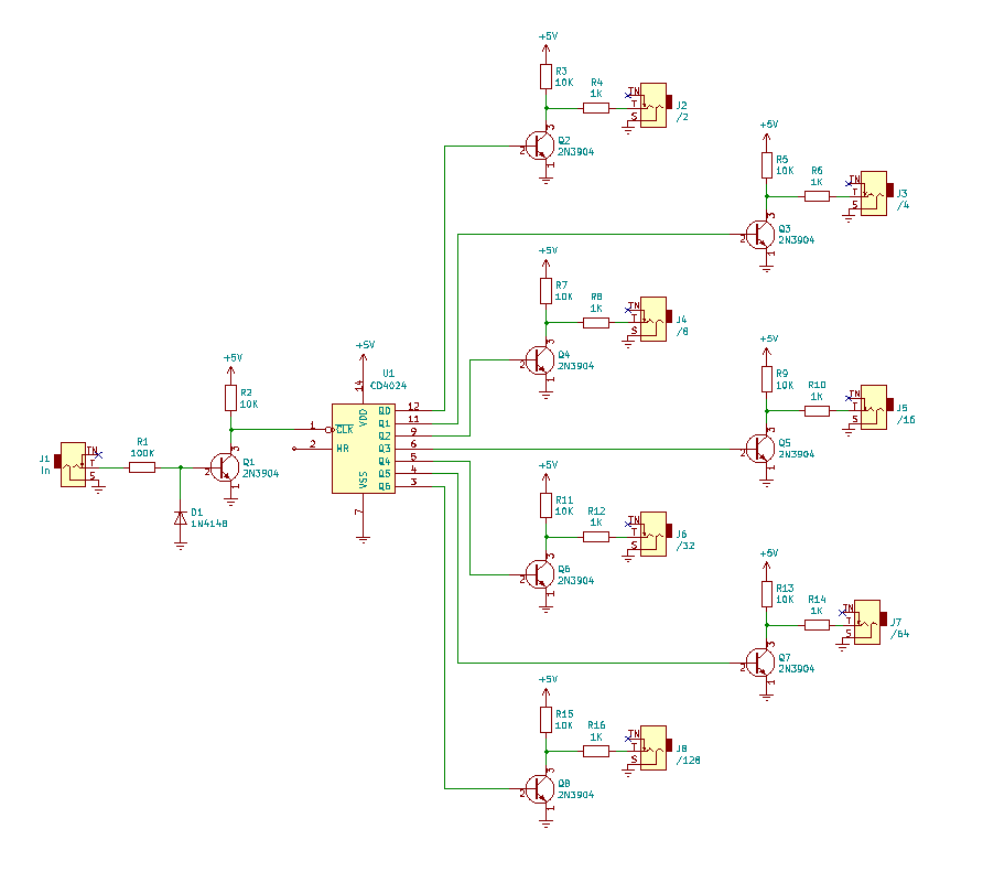
So this is what a CD4024 clock divider looks like at its most basic. Pretty simple! The resistor values really don't matter, I usually use 10K as a default and they worked well in this case. And since the CMOS outputs are so low current (~5mA max), we can omit resistors between the IC outputs and transistors.
The diode D1 is on the clock input to prevent negative voltages from damaging the transistor. They don't like it when the base is at a lower voltage than the emitter, it shortens their lifespan.
Now all we have left to deal with is the reset input. When it receives a voltage, it sets all outputs to be low. And while the reset is held high, it prevents the outputs from changing, basically acting as a "hold" input as well. Most synth clock dividers don't use the "hold" feature, and in fact put a gate-to-trigger converter on the reset input to prevent users from accidentally using it that way. I want to keep my options open, so I'll put in a gate-to-trigger converter, but I'll also include a jumper to bypass that if the user chooses.
The reset input is looking for a high gate - unlike the clock input. We don't want a NOT gate here, but we should still use a transistor to buffer the input. We don't want the IC to be damaged by all the weird voltages modular synths can produce, after all. Luckily, there is another equally simple circuit we can use: the gate buffer.

When the input is low, no current passes through the transistor and R2 acts as a pulldown resistor, setting the output to 0V. When the input goes high, current is allowed to pass through the transistor and the output is pulled up to 5V.
I mentioned earlier that I wanted to incorporate a gate-to-trigger circuit on the reset input, along with a jumper to bypass. You can make a gate-to-trigger with a simple RC high pass filter like this:

This will take a gate and turn it into a nice short trigger. Combining that with our transistor buffer, we get this:

So we've got components performing the following duties:
R1 providing 100K input impedance
D1 protecting the transistor from negative voltages
Q1 and R2 forming a gate buffer
C1 and R3 forming a high pass filter
And J1 is a 1x2 pin header that a jumper can fit over, to bypass the high pass filter
And when I soldered it all together.... it didn't work! An all too common experience. I probed around with the multimeter and it turns out that the transistor and the high pass filter each cause voltage drop, and the combination made the signal too weak for the CD4024 to register. So I reduced R1 to 47K, and added another buffer after the HPF, and lo and behold it worked!
With that, here is the fully functional clock divider:

This works, but it's still missing something: LEDs! No clock divider would be complete without blinking lights. Let's add an LED and resistor to the emitter of each output transistor, like this:
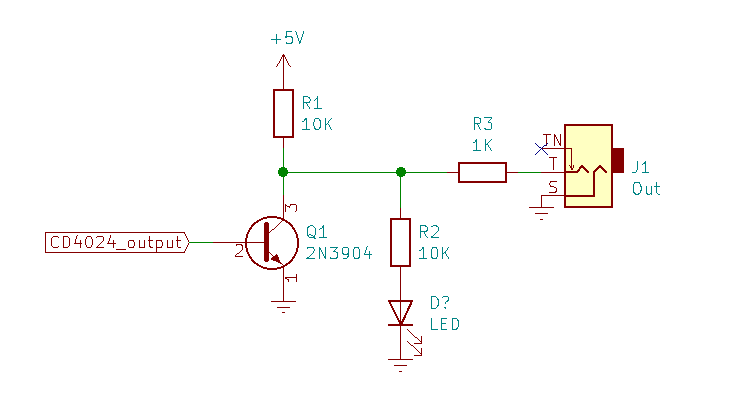
Unfortunately, R1 and R2 form a voltage divider here, so the output will only be 2.5V instead of the full 5V. We can work around this by decreasing R1's resistance - if we bring it down to 1K, then the output will be able to reach 4.5V. That's good enough for modular synths!
So incorporating the LEDs, we end up with this for the final design:

That's one clock divider down; let's check out another.
CD4017

There are ten outputs on this chip, numbered from 0 to 9. At any given time, nine outputs are low and one is high. With each pulse received at the clock input, the active output goes low and the next output goes high. The datasheet describes this chip as a "Decade Counter with 10 Decoded Outputs." Essentially, it is an IC that counts to ten.
This is super useful in a musical context. All you need to do is wire a pot to each output and you have a ten step sequencer. Hackaday has a great guide to building a "Baby 10" sequencer. On top of that, you can replace the pots with switches to make a simple trigger sequencer - or simply buffer the outputs to get individual gate outputs for each step.
You can also wire any output back to the reset input to create a shorter sequence. This is the feature we are going to exploit to create a clock divider.
When the reset input receives a pulse, output 0 immediately goes high and all other outputs go low; the sequencer is reset back to the first step. So if we connect the reset input to output 4 (for example), we will have a four step sequence.

When Out 4 goes high, the reset is triggered in under a millisecond - too fast to be perceptible. I drew it as a brief trigger in the diagram above just to illustrate what is happening, but it is too short to even be recognized as a trigger by most modules.
The result here is that the four active inputs (0 through 3) are now functioning as divide-by-four clock dividers, each one offset by a step. But I don't just want a divide-by-four clock divider, I want a module that will let me choose the division amount. All we need for that is a switch with a lot of positions.
This rotary switch will be just right for this project: it has eight positions, a small form factor, and a flatted shaft that fits the same knobs used on Eurorack pots. Here is the circuit with the switch included:

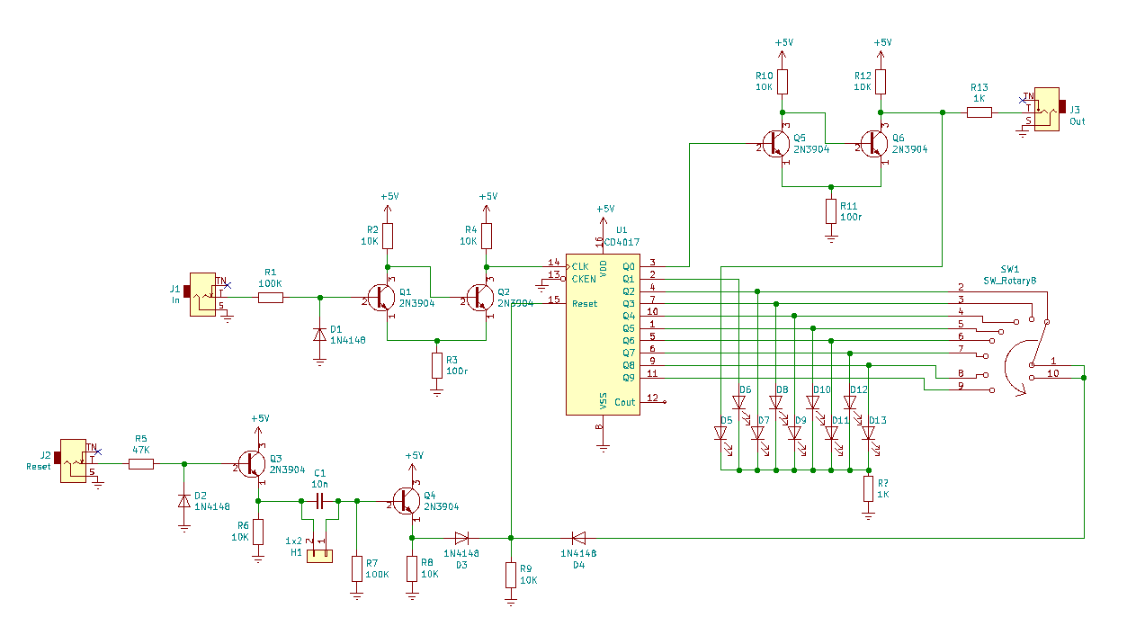
Output 0 is the output of our clock divider. I decided to leave Output 1 disconnected from the reset switch, as connecting that to Reset will result in a divide-by-1 clock divider, which I don't find useful. The way it is wired in the diagram above, we can select any value between divide-by-2 and divide-by-9.
There are two pins we won't be using, Clock Enable and Carry Out. Carry Out we can leave floating, and Clock Enable will be connected to ground. If Clock Enable is left disconnected, it can prevent the CD4017 from stepping through its outputs, essentially causing the circuit to freeze - so if you have a 4017 circuit on a breadboard and it isn't working, that's a good thing to check while troubleshooting.
Now that the core of the circuit is working, we need to add some input and output protections. Luckily, none of the inputs or outputs of the 4017 need to be inverted. However, they should still be buffered.
The Reset input can use the same circuit as the 4024's reset; buffer into gate-to-trigger converter (with jumper to bypass) into another buffer. We will need to add a diode OR gate to prevent voltage from the Reset input from being pushed into one of the 4017's outputs. The result looks like this:

The diodes D2 and D3 form the OR gate - they each allow current to flow towards the reset pin, but prevent current from flowing backwards towards Q2 or towards any of the 4017's outputs. CMOS ICs are fragile and do not like it when their outputs are on the receiving end of another voltage source.
For the Clock input, we will need a more robust buffer than the simple ones we used on the Reset input. We will be using a Schmitt Trigger instead.
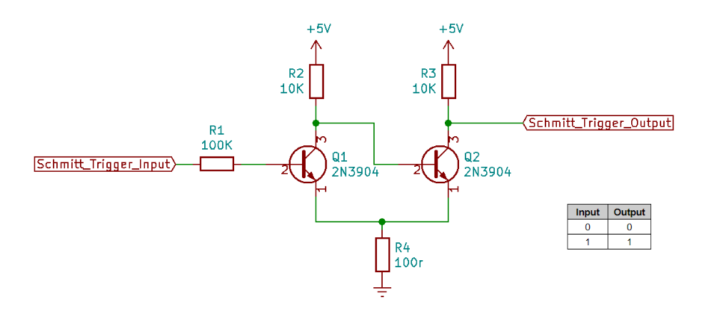
With a simple buffer, a noisy input will result in a noisy output. Schmitt Triggers smooth out the noise to produce a clean output. For a reset input, noise won't cause noticeable problems, but a noisy clock signal can cause your divider to become jittery and unpredictable.
The schmitt trigger above is a very simple one, it's just two NOT gates connected in series, with their emitters tied together. A double negative is a positive, so a NOT NOT gate is functionally the same as a buffer. Let's put one of these on the clock input as well as the divider output. This will ensure that the incoming clock is clean and at the correct voltage, and that the output has enough current to drive our other modules.

Couple of notes:
D1 is included to prevent negative voltage from damaging Q1
CMOS outputs are low current, so we don't need a resistor before Q5. We also don't need a diode there either, as there won't be any negative voltage present.
Now all that's left is to add the LEDs. Let's put an LED on each output of the 4017, that will create a pleasing "LED chaser" visual. We don't need one for Output 9, though. That last step will never be active in this circuit, since the 4017 is always being reset before it can finish counting to ten. So that's nine LEDs we will need to add. Also, since only one LED is ever lit at any given time, we can get away with using just one resistor for all these LEDs.
Final Thoughts
So why would we want to combine two clock dividers? Well, each circuit has its own inherent traits that can't be worked around. They each have pros and cons, and I feel like these two circuits balance each other out nicely.
CD4017
1 output
Can do odd & prime number divisions
Maximum division is 9
Output gates high for one clock cycle
Output can be controlled with knob
CD4024
7 outputs
Limited to power-of-two divisions
Can do super slow divisions
Output gates with 50% duty cycle
Outputs are fixed
Also, combining these two leads to some fun patching options. You can use the dividers in series to get suuuper slow divisions. You can also use one to reset the other for more complicated rhythms, similar to a Euclidean sequencer.
Something that the two circuits have in common, which is true of all CD40XX ICs, is that they are totally fine running at audio rate. That means you can use these as suboctave generators. With the odd-numbered divisions on the 4017, you can get harmonic intervals in between octaves. It can be a little glitchy and imperfect too, which to me is a huge bonus.
I tried to lay out the panel in an intuitive way, with only minimal text necessary. I was able to arrange the 4017's LEDs around the control knob, so whichever LED the knob it pointing to represents the last step before the counter is reset. The 4040 jacks and LEDs are all contained inside a graphic box, separated from the 4017 jacks, knob and LED.
After using it for a while, I noticed that I usually wanted the same clock to drive both dividers. So, I normalled the two inputs together. If a clock is patched to either input, it will be connected to both circuits. Of course, if two different clocks are patched to the inputs then the dividers will function independent of each other.
There a few features I would have liked to include - voltage control, or longer divisions with the 4017. These are definitely doable, but they would have required redesigning the entire thing from the ground up. I'm thinking of making another 4017-based clock divider down the road with those features. I'll keep you posted on that.
Full schematics are available for download below.